Chip Die Bonding Machines: A Complete Guide to Technology, Processes, and Applications
Chip die bonding is a semiconductor assembly process in which a small, individual piece of semiconductor material is attached to a supporting surface. This piece, called a die, contains electronic circuits that perform specific functions.
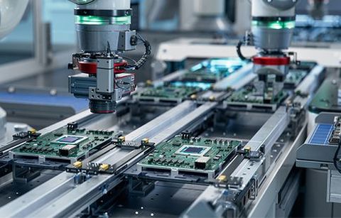
Before bonding, semiconductor wafers are processed and separated into individual dies. A die bonding machine then picks up a selected die, positions it accurately, and attaches it to a designated location.
The process is used in many electronic products, including smartphones, computers, automotive control units, communication equipment, sensors, and industrial automation systems.
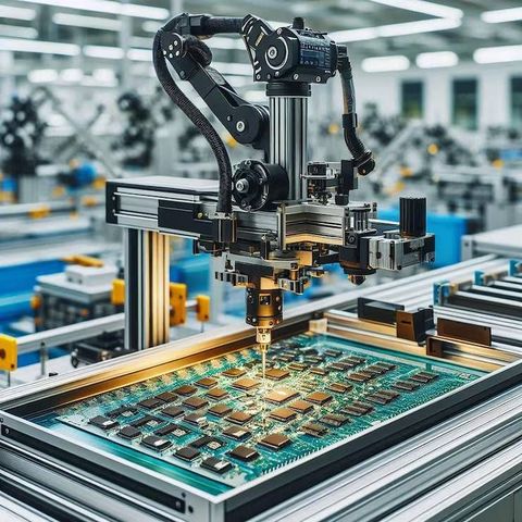
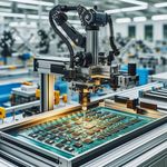
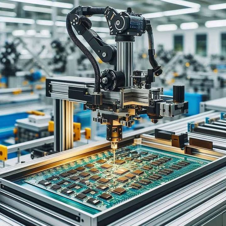
Modern chip die bonding machines combine mechanical positioning, optical inspection, temperature control, and automated handling. Depending on the application, they may use adhesive materials, solder, metal-based bonding layers, or other attachment methods.
The main objective is to create a stable connection between the semiconductor die and its supporting structure without damaging sensitive components.
Main Components of a Die Bonding Machine
A typical machine includes several coordinated systems.
Die pickup system: Collects individual dies from a wafer or carrier.
Vision system: Identifies die position, orientation, and alignment marks.
Placement mechanism: Moves the die to the required bonding location.
Bonding head: Applies controlled pressure, heat, or another bonding force.
Substrate handling system: Positions lead frames, circuit substrates, or packages.
Control system: Coordinates machine movements, process settings, and inspection results.
Quality monitoring system: Detects placement errors and certain bonding defects.
These components work together to support repeatable semiconductor assembly.
Why Chip Die Bonding Machines Matter Today
Importance in Modern Electronics Manufacturing
Electronic devices continue to become smaller while supporting more complex functions. This creates a need for accurate semiconductor packaging, where several components must fit into limited space and maintain dependable electrical connections.
Chip die bonding machines help manufacturers manage these requirements through controlled placement and repeatable attachment processes.
Their importance can be seen in several areas:
Miniaturization: Accurate die placement supports compact electronic assemblies.
Production consistency: Automated movements reduce variation between assembly cycles.
Advanced computing: Multi-die packages support processors designed for demanding computing workloads.
Automotive electronics: Reliable semiconductor packaging is important for control units, sensors, and power electronics.
Industrial automation: Semiconductor components support controllers, monitoring equipment, and communication systems.
Telecommunications: High-speed communication equipment depends on carefully assembled electronic components.
The machine's performance is only one part of the overall manufacturing process. Die quality, substrate preparation, bonding materials, temperature management, and inspection methods also influence the final result.
Industries That Use Die Bonding Equipment
The Main Bonding Process
The exact workflow depends on the machine design, die dimensions, bonding material, and package type. A typical automated process includes the following stages.
Wafer preparation: The semiconductor wafer is processed and separated into individual dies. The dies are inspected before assembly.
Die identification: An optical vision system locates the correct die and checks its orientation.
Die pickup: A pickup tool lifts the selected die from a wafer tape or carrier while minimizing mechanical stress.
Substrate alignment: The receiving surface is positioned, and the machine determines the required placement coordinates.
Die placement and bonding: The machine places the die and applies the specified bonding process, which may involve adhesive curing, solder reflow, or controlled heat and pressure.
Inspection: The assembly is checked for placement accuracy and visible defects. Additional testing may be required to confirm bond strength and electrical performance.
Common Types of Die Bonding Technology
Different applications require different bonding approaches. No single method is suitable for every semiconductor package.
Technology | How it works | Typical applications |
|---|---|---|
Epoxy die attach | Adhesive material secures the die to a substrate | General electronic packages and sensors |
Eutectic bonding | A suitable metal system forms a bond at a controlled temperature | Selected power and high-reliability devices |
Thermocompression bonding | Heat and pressure create a controlled bond | Advanced packaging and stacked dies |
Flip-chip bonding | The die is attached with its contact side facing the substrate | High-density electronic interconnections |
Hybrid bonding | Direct dielectric and metal connections join compatible surfaces | Advanced 3D integration and fine-pitch interconnects |
Hybrid bonding is particularly relevant to advanced semiconductor packaging because it can support dense interconnections between dies. However, it demands carefully prepared surfaces, precise alignment, and strong contamination control.
Important Machine Performance Factors
When assessing chip die bonding equipment, manufacturers typically consider several technical factors.
Placement accuracy: How closely the die reaches its specified position.
Throughput: The number of units processed over a defined period.
Repeatability: How consistently the machine performs the same operation.
Bonding force: Whether the applied force suits the die and attachment material.
Temperature control: Whether the bonding temperature remains within the process requirements.
Process monitoring: Whether the system records settings, detects faults, and supports traceability.
Performance should be evaluated under actual production conditions. A high nominal placement rate alone does not establish overall manufacturing quality.
Recent Developments in Die Bonding Technology
Advanced Packaging and Hybrid Bonding in 2025–2026
One major industry trend is the growing use of advanced packaging to combine multiple semiconductor dies in a single package. This approach can integrate processors, memory, and specialized computing functions without requiring every function to be manufactured on one monolithic chip.
In July 2025, industry reporting described increasing interest in hybrid bonding equipment for advanced memory and logic packaging. By 2026, hybrid bonding continued to receive attention as semiconductor manufacturers worked toward denser interconnections and three-dimensional integration.
Automation, Inspection, and Data Monitoring
Modern bonding systems increasingly combine vision inspection, automated material handling, and process data collection. These features help production teams identify alignment problems and investigate defects.
Important developments include:
Improved optical alignment for small dies and narrow interconnect spacing.
More integrated surface preparation and bonding workflows.
Data logging to support production traceability.
Automated inspection to identify placement and surface defects.
Greater attention to thermal management and material compatibility.
These improvements do not eliminate manufacturing defects. Their effectiveness depends on equipment configuration, process qualification, maintenance, and inspection standards.
Laws, Policies, and Manufacturing Standards
Semiconductor Equipment Safety Requirements
Chip die bonding machines operate in manufacturing environments that may involve moving mechanisms, heated components, electrical systems, adhesives, and specialized process materials. Appropriate safety controls are essential for protecting workers and maintaining stable production.
Applicable requirements depend on the country, equipment configuration, and manufacturing facility. Common areas of regulation include:
Machine safety: Guards, interlocks, emergency stops, and safe operating procedures.
Electrical safety: Protection against electrical hazards and appropriate equipment installation.
Chemical handling: Safe storage, ventilation, and handling procedures for adhesives, solvents, and cleaning materials.
Worker protection: Training, personal protective equipment, and controlled access to hazardous areas.
Environmental compliance: Proper handling of process waste, emissions, and industrial materials.
The SEMI S2 guideline addresses environmental, health, and safety considerations for semiconductor manufacturing equipment. Other SEMI guidelines cover ergonomics, electrical design, risk assessment, and environmental impact. These industry guidelines should be distinguished from legally mandatory requirements, which vary by jurisdiction.
In India, semiconductor assembly facilities must consider applicable factory safety requirements, environmental regulations, electrical standards, and chemical-handling rules. Government semiconductor initiatives also support the development of domestic manufacturing and packaging capabilities.
Other markets have their own regulatory frameworks. For example, equipment used in the European Union may need to comply with applicable machinery, electrical, and electromagnetic compatibility requirements.
Manufacturers should check current national laws, applicable technical standards, and facility-specific obligations before installing or operating bonding equipment. Compliance should be verified for the actual machine and production environment.
Tools and Resources for Learning About Die Bonding
Useful Technical Resources
Engineers, students, and manufacturing teams can use several general-purpose resources to understand semiconductor bonding processes.
CAD and process simulation tools: Help visualize die placement, substrate layouts, and equipment movements.
Optical inspection systems: Support alignment checks and detection of visible defects.
Temperature monitoring instruments: Help verify thermal conditions during bonding and curing.
Force measurement instruments: Help evaluate bonding pressure and mechanical consistency.
Statistical process control tools: Track process variation and identify unusual production patterns.
Maintenance checklists: Organize inspections, cleaning schedules, calibration, and preventive maintenance.
Semiconductor packaging textbooks: Explain die attachment, interconnections, materials, and reliability testing.
Manufacturing quality templates: Record process settings, inspection results, and defect classifications.
These resources help users understand how equipment performance is evaluated. Actual process settings should always follow validated manufacturing procedures and the equipment manufacturer's technical documentation.
Frequently Asked Questions
What is a chip die bonding machine?
A chip die bonding machine is equipment used to attach individual semiconductor dies to substrates, lead frames, or other supporting structures. It uses controlled positioning and a suitable bonding method to create a stable assembly.
What is the difference between die bonding and wire bonding?
Die bonding attaches the semiconductor die to its supporting structure. Wire bonding connects electrical contact points using fine metal wires. Both processes may be used in the same semiconductor package, although some advanced packages use alternative interconnection technologies.
Which industries use chip die bonding machines?
The main applications include semiconductor manufacturing, consumer electronics, automotive electronics, industrial automation, telecommunications, power electronics, and advanced computing. The appropriate equipment depends on the component design and production requirements.
Why is alignment accuracy important in die bonding?
Incorrect alignment can affect electrical connections, package dimensions, thermal behavior, and product reliability. Accurate placement becomes especially important when dies contain many closely spaced contacts or when multiple dies must be integrated into one package.
What is the future of chip die bonding technology?
Future developments are likely to emphasize advanced packaging, hybrid bonding, three-dimensional integration, automated inspection, and improved process monitoring. The pace of adoption will depend on technical qualification, manufacturing requirements, and the needs of individual semiconductor applications.
Conclusion
Chip die bonding machines play an important role in transforming semiconductor dies into functional electronic assemblies. Their performance depends on precise placement, suitable bonding materials, controlled process conditions, and effective inspection.